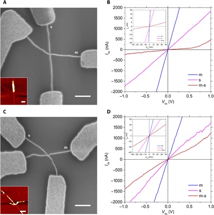
Fig. 5. Layout and performance of SWCNT FETs.

(A and C) SEM images of two representative SWCNT FETs without (A) and with (C) the carbon-welded joint. Scale bars, 1 μm. The inset AFM images show the deposited carbon (white part) on the SWCNTs. Scale bars, 100 and 200 nm, respectively. (B and D) Ids versus Vds of the device (A) and (C), respectively. Gate voltage Vgs = −10 V.
