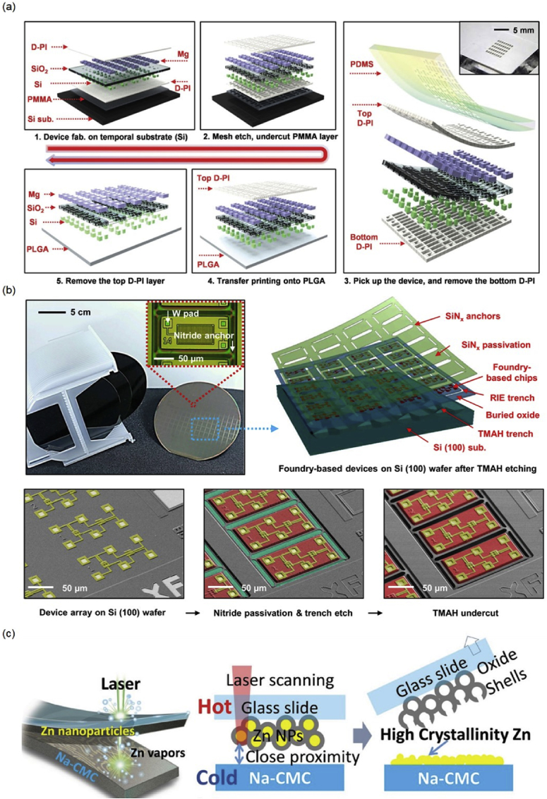
Fig. 3.
(a) 2-step transfer printing procedure of transient electronic circuits: (upper left) defining a mesh type structure allowing the undercut of sacrificial PMMA layer to release the entire device (upper middle), retrieving the released device onto a PDMS stamp (right) followed by the removal of the bottom D-PI layer, transfer printing onto a PLGA substrate (lower middle), and final RIE etching of the top D-PI layer (lower left); (b) Device configuration and release procedures of wafer-scale, ultrathin silicon components for transient electronics. The bottom individual frames correspond to: (left) the unprocessed wafer (device arrays colored with gold), (center) the wafer after passivation and trench etching (the released region of individual device blocks colored with red, and the underlying silicon (100) handle wafer colored with cyan), and (Right) the wafer after TMAH undercut etching; (c) Schematic illustration of evaporation-condensation-mediated laser printing: (left) irradiation of pre-coated Zn NPs (2.5–5 μm) by a high speed scanning laser, (center) glass slide with Zn NPs gently pressed on to the Na-CMC substrate for laser irradiation, (right) Zn conductors with high crystallinity obtained on the Na-CMC substrate. Reprinted with permissions from Refs. [17, 30, 42].

