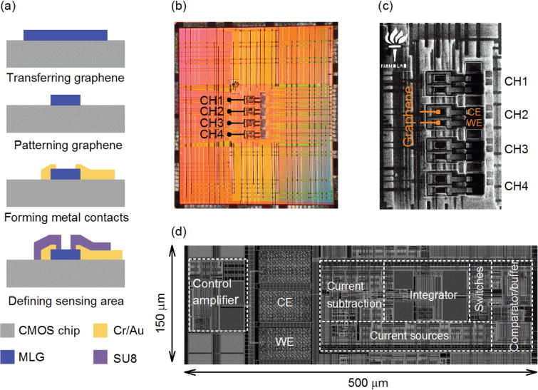
Fig. 8.

(a) Schematic illustration of the key post-processing steps for constructing the MLG sensor array above the CMOS chip. (b) Micrograph of the CMOS-graphene prototype chip. (c) Top-view SEM image of the post-processed chip, illustrating the MLG sensor array. (d) The illustration of the circuit layout of a readout channel. The size of the CMOS channel is 150 μm× 500 μm.
