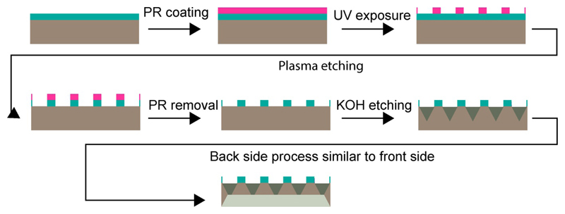
Figure 1.
Fabrication scheme for the crystallography chip. The process starts with conventional UV lithography to transfer the pattern of loading sites to a silicon wafer (gray, with a layer of silicon nitride, SiN, in cyan) coated with photoresist (pink). The pattern is then transferred to the SiN layer using reactive ion etching and the photoresist is stripped. The SiN layer plays the role of the mask for wet etching in the subsequent steps. KOH etching results in a trapezoidal shape that enhances loading efficiency. The same procedure is repeated for the back side of the chip to make it thin enough to fit a specific size of crystals.

