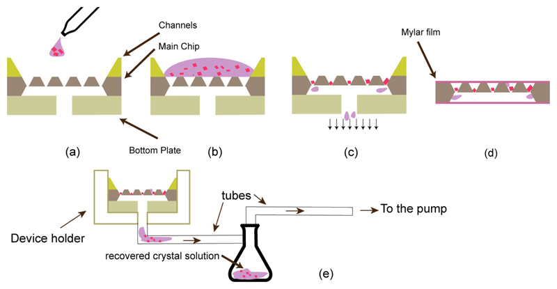
Figure 4.
(a, b, c) Chip loading scheme with chip components designed for crystal solution loading. The silicon piece with channels is placed on top of the chip for guiding crystal solution into the compartment rows. The bottom plate helps to apply effective negative pressure for trapping the crystals in features (c). (d) The loaded chip is wrapped in a thin film of mylar to avoid crystal dehydration. The crystal solution removed from the chip can be collected in an additional reservoir for use with a different chip size (e). All figures are schematics and are not to scale.

