
Fig. 4. Toward 2D quantum-well superlattice with atomically sharp lateral interfaces.
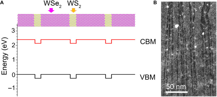
(A) Atomic structural model and band alignment for a WSe2/WS2 superlattice calculated with the HSE06 functional. Valence band maximum (VBM) and conduction band minimum (CBM) are plotted by black and red lines, respectively. Yellow, S; purple, Se; gray, W. (B) Low-magnification STEM-ADF image showing the formation of parallel MoS2 quantum wells of a few hundred nanometers long in a MoSe2 monolayer toward the formation of quantum-well superlattice.