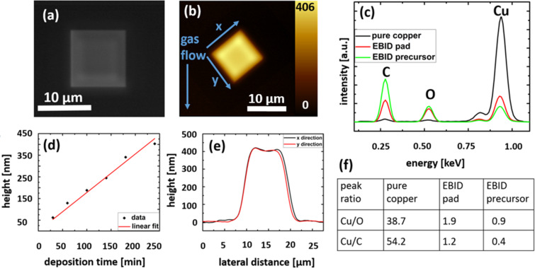
Figure 1.
(a) Scanning electron micrograph of a FEBID pad. (b) Atomic force micrograph of the same pad. (c + f) EDX spectra of the solid crystalline precursor, a copper foil with a purity >99.999% and a FEBID pad grown on a silicon substrate with a height above 400 nm. The table shows the peak ratios of copper to oxygen and copper to carbon (d) Height of FEBID pads for different deposition times, written with a dwell time of 10 μs and a point distance of 3 nm. (e) Atomic force microscope line scans of the FEBID pad in (a) and (b).

