
Fig. 2. Operation and design of the NN-Chip platform.
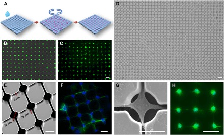
(A) Schematic of the cell loading process. (B) Representative image of loading efficiency. The 661W cells were incubated in the medium with calcein for 20 min before loading. (C) Cell morphology after incubation for 1 hour on chip after loading. Scale bar, 40 μm. (D) Results of large-area loading by using the MDA-MB-231 cells with optimized parameters. Scale bar, 40 μm. (E) A scanning electron microscopy (SEM) image shows the neural network structure, including the microwells and their connecting microchannels, of the NN-Chip at a 30° tilt angle. (F) Representative images show that the 661W cells formed neural network on the NN-Chip. The actin (green) was labeled by phalloidin, and the nuclei (blue) was labeled with 4′,6-diamidino-2-phenylindole (DAPI). (G) A representative SEM image shows a 661W cell with synapses extending into the surrounding chambers along with the microchannel. (H) Neural network created by iCell neurons. Cells were stained by calcein after culturing on chip for 12 hours. Scale bar, 20 μm.