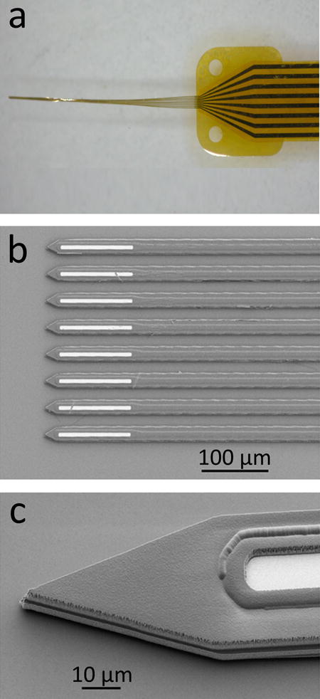
Figure 6.

An 8-channel a-SiC microelectrode array (MEA) developed using standard semiconductor fabrication processes. The MEAs are fabricated on a thin layer of polyimide which is spin-coated on a silicon carrier wafer. After fabrication, the carrier wafer is soaked in deionized water to release the devices. a, When withdrawn from deionized water, the shanks of the a-SiC MEA forms a bundle. b, optical micrograph showing the electrode sites at the distal end of the array. Electrode openings are created by reactive ion etching. c, scanning electron micrograph showing the tip profile with a near-vertical sidewall created using an inductively coupled plasma etching system.
