
Fig. 4. Photon energy scaling for interband heating.
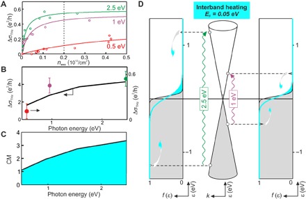
This figure is analogous to Fig. 3, with the difference that the measurements are done at Vg = 0.5 V, the point of lowest DC conductivity (σ0 ≈ 2 e2/h), corresponding to graphene close to the charge neutrality point. The calculations are done for EF = 0.05 eV, although because of puddles, the effective Fermi energy in the experiment could be significantly larger. We observe that the value of the THz photoconductivity is positive, whereas in Fig. 3, it is negative. (A and B) The THz photoconductivity for three pump photon energies Eph = 0.5, 1.0, and 2.5 eV. (C) The calculated CM factor, defined in the main text. Interband heating contributes to the broadening of the electron distribution, shown in (D). The broadening of the electron distribution is larger in the Eph = 2.5 eV case, indicating more interband heating for larger photon energy. To understand the magnitude of the photoconductivity, we note that the added carrier density in the conduction band corresponds to Δn = CM⋅ nexc. Using CM = 3 (for a photon energy of 2 eV), nexc = 0.2⋅ 1012/cm2, and a mobility of μ = 1000 cm2/Vs, we obtain an increased conductivity of Δσ = Δneμ = 4 e2/h. This agrees with the calculated increase in conductivity (see Fig. 4B for a photon energy of 2 eV). The measured value is significantly lower, most likely due to electron-hole puddles.