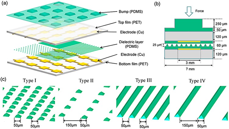
Figure 3.
(a) Schematic diagram of the capacitive tactile sensing array; (b) cross-section view of one sensing unit; (c) schematic diagram of different geometries of the microstructures on the polydimethylsiloxane (PDMS) layer. Reprint from [89], copyright (2016), with permission from MDPI AG.

