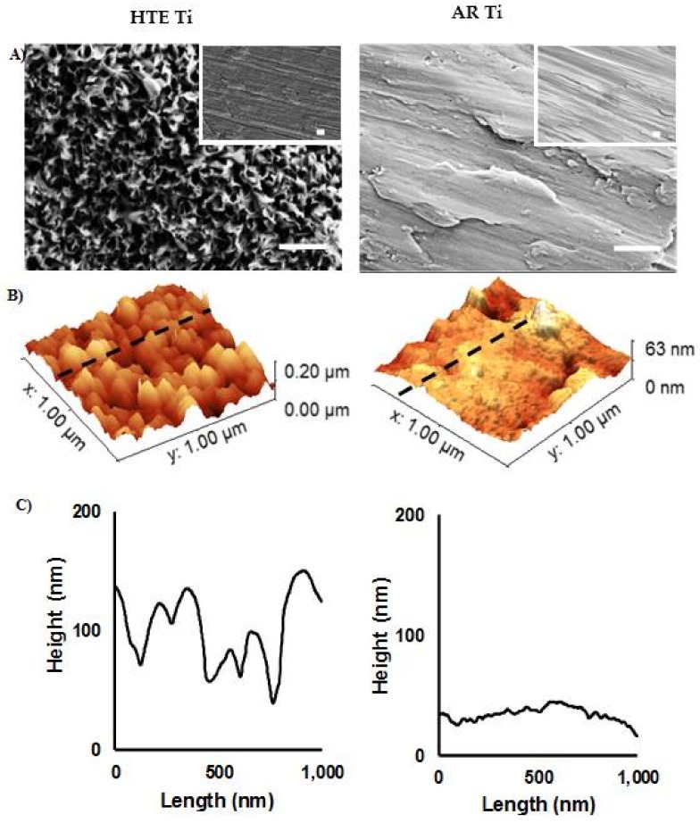
Figure 1.
Surface topographic characterisation of as-received and nanostructured titanium. (A) SEM images of the surfaces of AR (right) and HTE Ti (left) (scale bar = 400 nm). Insets are images taken at 5000× (scale bar = 2 µm). (B) Typical 3D AFM images and (C) corresponding surface profiles of AR and HTE Ti surfaces over 1 × 1 µm2 scanning areas, showing a significant change in surface nanoarchitecture resulting from the hydrothermal treatment.

