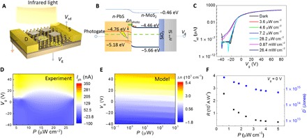
Fig. 1. Schematic and optoelectronic transport of infrared memory device.

(A) Schematic of infrared memory device, showing few-layer MoS2-PbS nanoplates heterostructure connected to source (S) and drain (D) electrodes. Infrared light entirely illuminates the device. (B) Band alignment of heterostructure. The photogate effect is schematically presented on the PbS side. (C) Transfer characteristic curves of Isd versus Vg under infrared illumination with variable light power density P. (D) Vg- and P-dependent photocurrent Iph extracted from transfer characteristic curves in (C). (E) Numerical simulation of carriers density (Δn) in MoS2 channel via photo injection and Vg injection. (F) Dependence of responsivity and specific detectivity on power density shows maximum R of 2.6 × 10⁷ A/W and D* of 5.5 × 10¹⁵ Jones at P = 0.6 mW cm−2.
