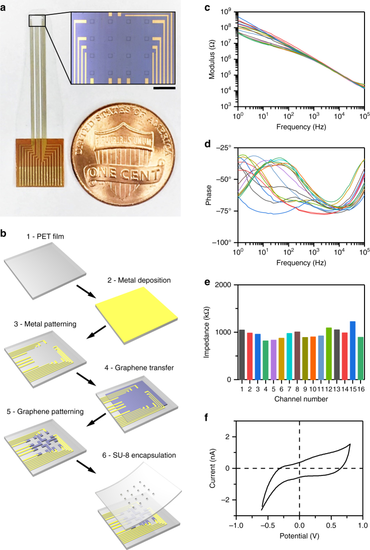
Fig. 1.
Graphene microelectrode array fabrication and electrochemical characterization. a Design of the graphene microelectrode array. Each electrode is a 100 µm×100 µm square and the spacing in-between two adjacent electrodes is 300 µm (edge-to-edge). Scale bar, 500 µm. b Fabrication of graphene microelectrode arrays. Step 1: clear 50 µm-thick PET film. Step 2: 10 nm Cr and 100 nm Au sputtered onto the PET film. Step 3: metal wires patterned with photolithography and wet-etching. Step 4: graphene transfer with bubbling method. Step 5: graphene contact pads patterned with photolithography and oxygen plasma-etching. Step 6: spin-coating of SU-8 and patterning of openings with lithography. c, d Electrochemical impedance spectroscopy of all 16 channels on an array. e Impedance at 1 kHz; channels have an average impedance of 963 kΩ. f Cyclic voltammetry of a representative channel shows no redox peaks

