Fig. 1.
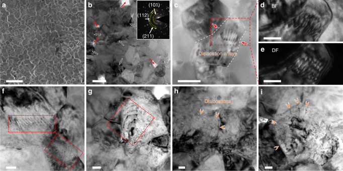
Microstructure of flash-sintered 3YSZ. a SEM images of the unpolished flash-sintered 3YSZ. The average particle size is ~1 μm. Scale bar, 3 μm. b Bright-field TEM micrograph showing subgrains with grain boundaries and defects generated during flash sintering (labeled by black arrows), and nanopores (~1.4%) (indicated by red arrows). The inserted SAD pattern shows diffraction rings. Scale bar, 200 nm. c A STEM micrograph showing a dislocation array inside a grain in the flash-sintered 3YSZ. The dislocation array was generated in a bottleneck region of the grain as indicated by red arrows. Scale bar, 100 nm. d, e Bright-field (BF) and dark-field (DF) TEM micrographs showing the dislocation array in the boxed region in c. Scale bar, 50 nm. f–i Numerous BF TEM images of the flash-sintered 3YSZ showing the existence of dislocations and dislocation arrays in grains. Scale bar, 50 nm

