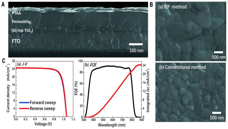
Figure 11.
SEM observations and J-V and EQE measurements. (A) Cross-sectional FESEM image of the device; (B) The comparison of FESEM surface images of FAPbI3-based layer formed on mp-TiO2 by IEP and conventional method. (C) (a) J-V curves of best device measured with a 40-ms scanning delay in reverse (from 1.2 V to 0 V) and forward (from 0 V to 1.2 V) modes under AM 1.5G illumination and (b) EQE spectra for best device and integrated JSC (Reprinted with permission) [15].

