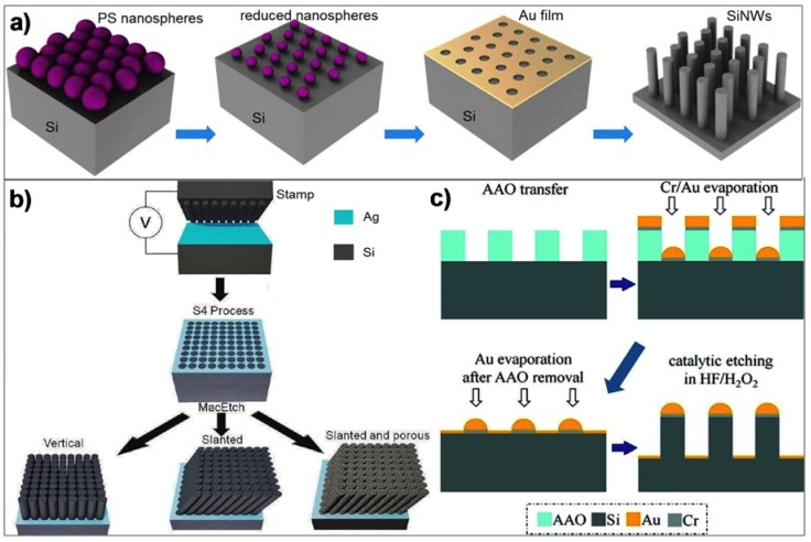
Figure 2.
(a) Schematic of a typical vertical SiNWs’ fabrication process based on blocking-dots patterning. Polystyrene (PS) nanospheres are deposited on Si wafer, followed by gold (Au) deposition. The resulting Au mesh serves as catalytic mask in the etchant solution (e.g., H2O/HF/H2O2) to define the SiNWs, Reprinted with permission from Ref. [34], Copyright (2011), IOP. (b) Vertical SiNWs fabrication by ionic solid-state molding. SiNW pattern is transferred from an Ag2S stamp onto an Ag coated Si wafer by applying a potential. Such pattern is used for catalytic wet-etching to form the SiNW, Reprinted with permission from Ref. [39], Copyright (2010), ACS. (c) Fabrication of vertical SiNWs by anodized aluminum oxide (AAO) molding. An AAO mold with desired pore diameters is used as a shadow mask for patterning of Au/Cr blocking-dots, which later will be used to define SiNWs through a catalytic wet-etching. Reprinted with permission from Ref. [33], Copyright (2010), ACS.

