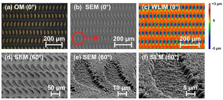
Figure 9.
Top-view: (a) optical micrograph; (b) SEM micrograph; and (c) WLIM topography of hybrid micro-nanostructures processed on Ti6Al4V-alloy (φ0 = 0.25 J/cm2; Neff_1D = 600, λ = 790 nm, τ = 30 fs, f = 1 kHz, w0 ≈ 73 µm, line separation Δy = 90 μm, area 7 × 7 mm2). The red circle in (b) indicates the Gaussian beam diameter D for comparison. The red arrow marks the direction of line scanning which is parallel to the laser beam polarization. The lower row (d–f) displays detailed magnifications taken under 60° by SEM.

