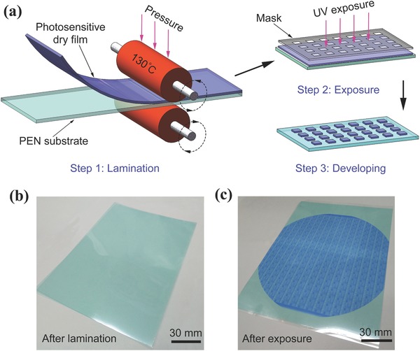
Figure 1.

Device fabrication based on a photosensitive dry film. a) Schematic of the lamination and patterning processes of a dry film on a flexible substrate: step 1, a dry film is laminated onto a PEN substrate by a roll‐to‐roll technique under optimized temperature and pressure conditions; step 2, UV exposure of the dry film through a mask pattern; and step 3, the pattern is formed after a developing process. b,c) Photographs of real devices in A5 paper size showing views after lamination and after exposure.
