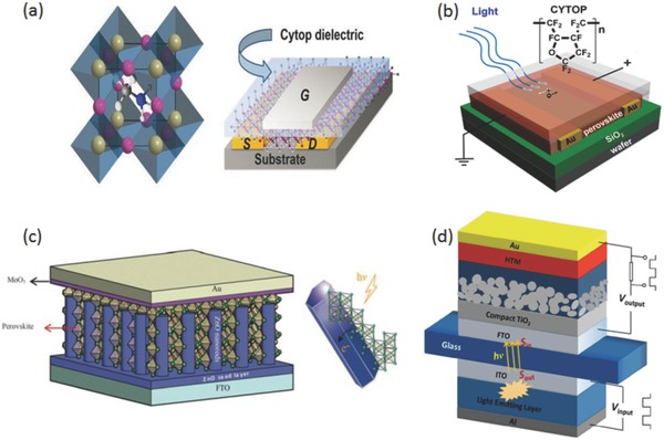
Figure 8.

a) The schematic structure of the FETs on hybrid halide semiconductor layer, having Au source and drain contacts, Cytop dielectric, and Al gate electrode. Reproduced with permission.135 Copyright 2015, Cambridge University Press. b) The structure of photodetector with a layer of fluorous polymer coating which can increase the lifetime of the device. Reproduced with permission.62 Copyright 2015, American Chemical Society. c) Schematic diagram and energy level diagram of the as‐fabricated perovskite photodetector. Reproduced with permission.137 Copyright 2016, Published by The Royal Society of Chemistry. d) The schematic diagram of an organic–inorganic hybrid optocoupler. Reproduced with permission.139 Copyright 2015, Nature Publishing Group.
