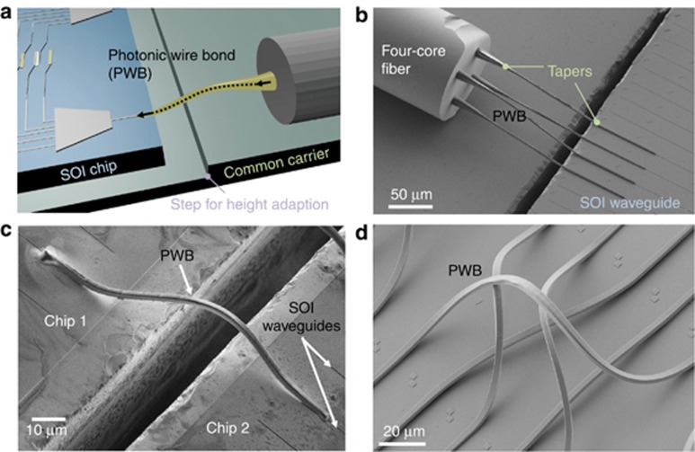
Figure 8.
PWB by the 3D DLW lithography approach121, 122. (a) A principal scheme of the PWB enabling connection of an SOI chip with an optical fiber. (b) A four-core optical fiber coupled with SOI waveguides by tapered photonic wires. (c) An integrated chip with two SOI waveguides coupled together via freeform PWB; note a spatial (lateral) displacement of the SOI waveguides on the separate chips. (d) An example of 3D PWB capability enabling virtually direct signal transferring through different communication platforms. Images courtesy of Prof. C. Koos. (2015) IEEE. Reprinted, with permission, from Ref. 122.

