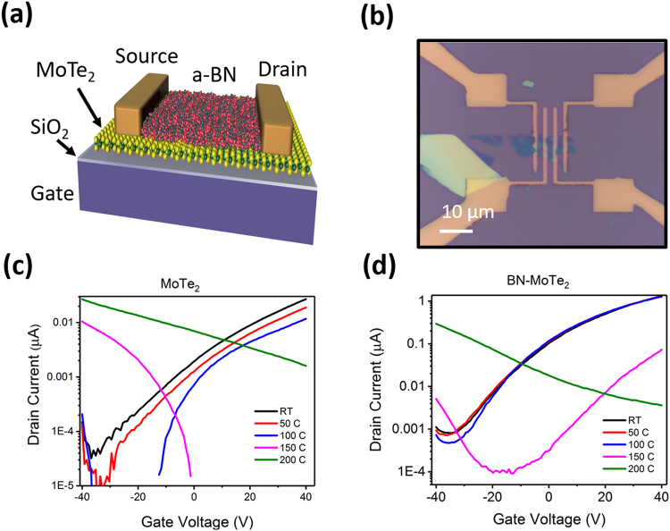
Figure 4.
(a) Schematic cross-section of FET back-gated device with BN capped MoTe2. (b) Optical image of typical MoTe2 few-layer flake with Ti/Au source drain contacts deposited by EBL. (c) Examples of drain current measurements as a function of gate voltage for a backdated MoTe2 device. The drain voltage was maintained at 1 VDC. Uncovered MoTe2 device shows initial n-type semiconducting behavior that switches to p-type after 150 °C. (d) The BN/MoTe2 device maintains a much greater degree of stability through 100 °C and exhibits a polarity switch to p-type behavior much later at 200 °C.

