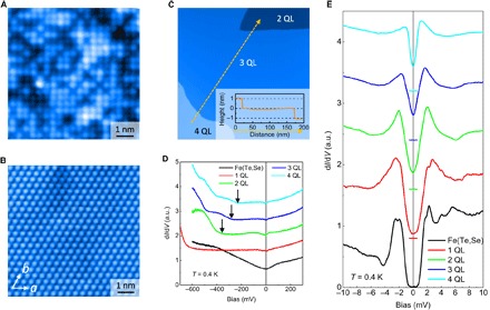
Fig. 1. STM/STS characterization of Bi2Te3/FeTe0.55Se0.45 heterostructure.

(A and B) Atomically resolved topography (with bias voltage Vbias = 10 mV and tunneling current It = 200 pA) of the (A) FeTe0.55Se0.45 substrate and (B) 2-QL Bi2Te3 thin film. The measured lattice constants of the top Te/Se surface on FeTe0.55Se0.45 with square lattice and Te surface on Bi2Te3 with hexagonal lattice are 3.80 and 4.38 Å, respectively. Using a deposition rate of about 0.5 QL/min, we obtain the Bi2Te3 thin film with very good connectivity. The thickness changes from place to place. (C) Topographic image (Vbias = 2 V, It = 10 pA, 150 × 150 nm2) of Bi2Te3 film with different thicknesses. The height difference for each step along the dashed yellow arrowed line is about 1.0 nm, which equals a thickness of 1 QL. (D) Typical differential conductance spectra (set-point bias voltage Vset = 0.45 V, Iset = 300 pA) measured on FeTe0.55Se0.45 substrate and Bi2Te3 thin films with different thicknesses. The black arrows show the positions of the typical kink features probably from the Dirac point of the Bi2Te3 films of different thicknesses. (E) Tunneling spectra with SC feature (Vset = 10 mV, Iset = 50 pA) measured on FeTe0.55Se0.45 substrate and 1- to 4-QL Bi2Te3/FeTe0.55Se0.45. The short horizontal bars with the same color mark the zero differential conductance for each curve. The typical feature of the spectra on the FeTe0.55Se0.45 substrate is that one or two pairs of coherence peaks can be observed with peak energies varying from 1.1 to 2.1 meV. The tunneling spectrum measured on 1-QL Bi2Te3 also has the trace of coherent peaks of FeTe0.55Se0.45. This feature is absent on the 2-QL or thicker Bi2Te3 films. a.u., arbitrary units.
