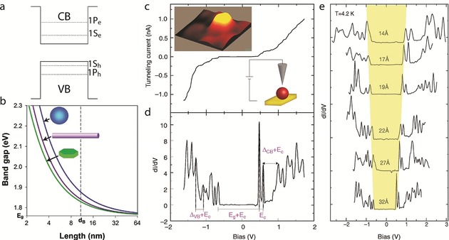
Figure 3.

a) Schematic diagram of the conduction and valence band structure in a CQD. b) Effect of the shape on the electronic properties of SCNCs. The diagram presents the Eg value of CdSe quantum wells, wires, and dots, as a function of the length of the confined dimension. The dotted line represents the exciton Bohr radius. Reprinted from Ref. 60 with permission. c) Tunneling I‐V curve of InAs QDs exhibiting single‐electron tunneling effects. The left inset presents a 10×10 nm2 STM topographic image of the QD. The right inset shows a schematic illustration of the STM measurement; the QD is linked to the surface, while the tip is positioned above the QD. d) Tunneling conductance spectrum (dI/dV versus V). The arrows indicate the main energy separations: Ec is the single‐electron charging energy, Eg is the nanocrystal band gap, and ΔVB and ΔCB are the spacings between levels in the valence and conduction bands, respectively. e) STS spectra of a size series of InAs CQDs. As the size of the CQD is decreased, the energy gap increases. (c)–(e) reprinted from Ref. 62 with permission.
