Fig. 1.
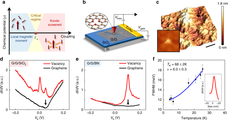
Kondo peak at a single-atom vacancy in graphene. a Schematic phase diagram of the pseudo-gap Kondo effect. The critical regime (yellow) separates the Local-magnetic-moment phase from the Kondo-screened phase. Arrows represent the ground state of the system with the large arrows corresponding to the local spin and the smaller ones representing the spins of electrons in the conduction band. b Schematics of the experimental setup. c STM topography of a double layer graphene on SiO2 (G/G/SiO2). The arrow indicates an isolated vacancy (Vb = −300mV, I = 20pA, Vg = 50 V). The scale bar is 20 nm. Inset: atomic resolution topography of a single atom vacancy shows the distinctive triangular structure (4 nm × 4 nm), Vb = −200mV, I = 20pA, Vg = −27V. d dI/dV spectra at the center of a single atom vacancy (upper red curve) and on pristine graphene far from the vacancy (lower black curve). The curves are vertically displaced for clarity (Vb = −200mV, I = 20pA, Vg = 0 V). The arrow labels the Dirac point. e Same as d but for a vacancy in a G/G/BN sample (Vb = −200mV, I = 20pA, Vg = −30V). f Evolution of the measured full width at half maximum (FWHM) of the Kondo peak with temperature (black data points) shown together with the fit (blue solid line) discussed in the text. Error bars represent the linewidths uncertainty obtained from fitting the Kondo peak to a Fano lineshape. Inset: Zoom into the Kondo peak (black dotted line) together with the Fano lineshape fit (red solid line)

