
Fig. 4.
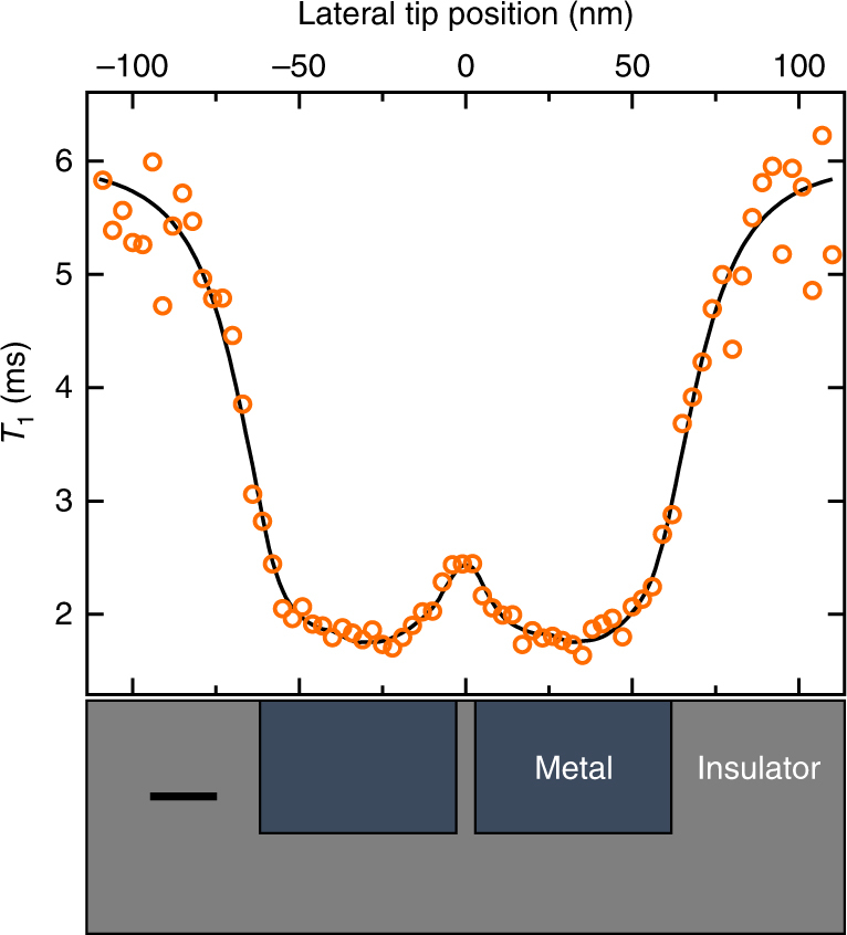
Simulated NV T1 line scan taken across a Mott insulator. The Mott insulator contains conducting pockets in an insulating material, as shown schematically at the bottom of the figure. The conducting regions, with σ = 3 × 10³ Ω−1 cm−1, are 40 × 40 × 60 nm3 in size and are separated by 5 nm. Scale bar is 20 nm. The black curve is the theoretical T1 and the orange circles represent a simulated measurement using spin-to-charge readout with 1 min of averaging per point. The NV-metal separation is 5 nm and the intrinsic NV T1 is 6 ms