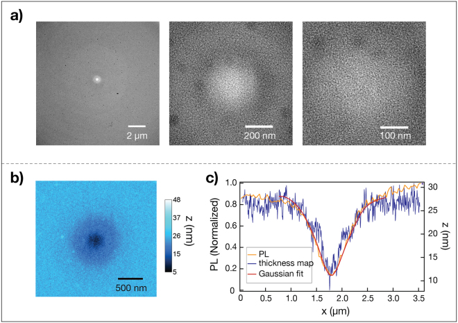
Figure 3.
Thickness characterization of a laser-etched spot. (a) TEM images at 195×, 39000× and 75000× (left to right). The lighter region corresponds with higher transmittance and thus thinner material. (b) TEM thickness map of an etched spot in nanometers. (c) Blue curve- TEM thickness map. Purple curve- normalized photoluminescence (PL) scanned in the x direction with a 30 nm step size. Red curve- simulated normalized PL based on a convolution of a diffraction-limited Gaussian, representing the laser beam, with the TEM thickness map.

