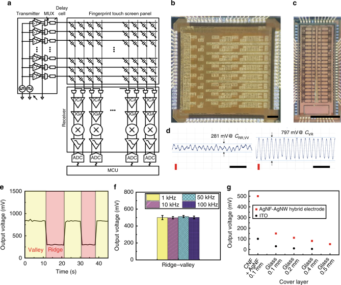
Fig. 4.
Custom-designed fingerprint sensor readout circuit. a Block diagram of the fingerprint sensor readout circuit. b Fully differential receiver for fingerprint recognition. Scale bar is 250 μm. c High-voltage transmitter. Scale bar is 1 mm. d Measurement result of the sensing ridge to the valley indicated the analog voltage outputs of the proposed IC and the fingerprint TSP (1 MHz, 1 V). Output voltages are 281 and 797 mV under ridges and valleys. Y-axis scale bar (red) is 200 mV and the x-axis scale bar (black) is 2 μs. e Waveform output voltage change during the fingerprint sweep. f Output voltages of the fingerprint sensor depend on fingerprint ridges and valleys with different noise frequencies. g Comparison of output voltages of the fingerprint sensor using a silver nanofiber (AgNF)–silver nanowire (AgNW) hybrid versus indium thin oxide (ITO) electrodes with different thickness of glass cover layers and a cellulose nanofiber (CNF) + AgNF cover layer

