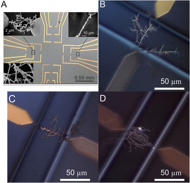
Figure 2.

(A) Optical microscopy image of a 13 × 13 mm chip with contact paths and growth electrodes structured by photolithography, and the nanowire electrodes assembled by DENA (contact pads are not shown on the image). Inserts in (A) show SEM images of Pd-Au (up left), Pd (up right), and the structural features of an Au (below) nanowire electrodes prepared by DENA. Optical microscopy images of Au (B), Pd (C), and Pd-Au (D) nanowire, and nanodendrite electrodes prepared by DENA after isolation with polyimide polymer.
