
Fig. 1. Design of the quantum dot crossbar array.
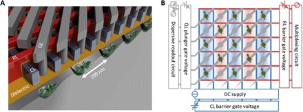
(A) Three-dimensional model of the array gate structure. The dielectrics in between the various gate layers are left out for clarity. (B) Schematic representation of the 2D quantum dot array. CLs (blue), RLs (red), and QLs (gray) connect the qubit grid to outside electronics for control and readout. A combination of these lines enables qubit selectivity. In the state shown here, half of the quantum dots are occupied with a single electron, where the electron spin encodes the qubit state. The electrons can be shuttled around via the gate voltages, providing a means to couple to nearest neighbors for two-qubit logic gates and readout and to couple to remote qubits for long-range entanglement.