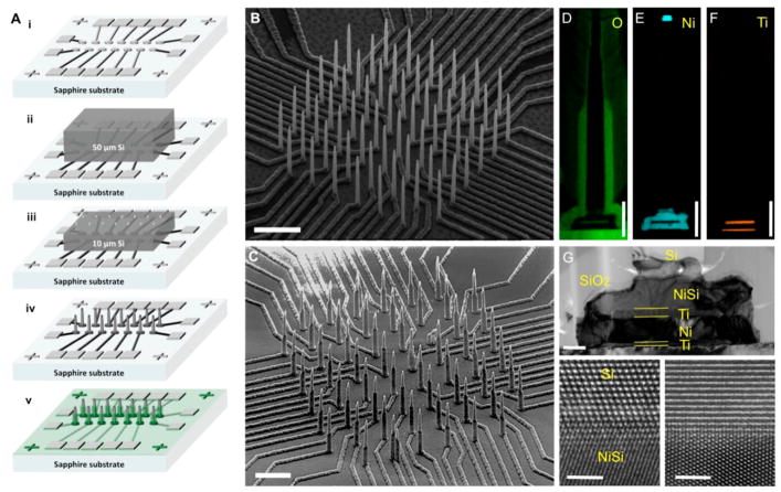
Figure 1.
(A) Illustration of fabrication procedure for high density electrically isolated nanowire probes by solid-state wafer bonding. (i) Metal stack with Ni topmost layer is patterned by a combination of photolithography and electron beam lithography atop an electrically insulating and transparent sapphire substrate. (ii) Si is bonded to the substrate in i by nickel silicidation. (iii) Si wafer is thinned down to the desired wire height. Ni masks are then defined by electron beam lithography and aligned to the bottom plane Ni pattern. (iv) Si nanowires are etched by an SF6/C4F8 plasma etch step. (v) SiO2 PECVD is then deposited and is selectively etched to expose the tips of the Si nanowires. (B, C) SEM images of an 8 × 8 Si nanowire array (B) after etching and (C) after SiO2 passivation. Scale bar in B is 5 μm and in C is 3 μm. (D, E). Energy-dispersive X-ray spectroscopy (EDX) of the (D) oxygen signature of the SiO2 passivation layer, (E) nickel for etching mask (top), NiSi region, and conducting lower most layer, and (F) Ti as the diffusion barrier (top) and adhesion layer (bottom). Scale bars are 1 μm. (G) High magnification TEM image of the NiSi/Ti/Ni/Ti underneath the Si nanowire highlighting the interfacial structure between the bottom conducting lead and the Si nanowire. Scale bar is 200 nm. The bottom panels are HRTEM images at the interface between Si and NiSi with electron beam axis aligned in the Si [1̄10] (left panel), and the NiSi [1̄10] Zone axis in (right panel) to display the crystalline interface. Scale bars in bottom panels are 2 nm.

