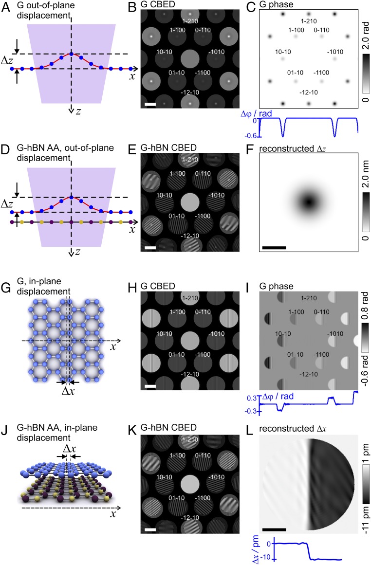
Fig. 3.
Simulated CBED patterns for graphene and graphene–hBN bilayer heterostructures where graphene lattice is deformed. (A) Side view illustration of a graphene layer with atoms displaced out of plane, not drawn to scale. (B) Corresponding simulated CBED pattern where the atoms are displaced out of plane in the form of a bubble. The atomic z positions are shifted by Δz = −ABexp[−(x2 + y2)/(2σ2Β)], AB = 2 nm, and σΒ = 2 nm. (C) The difference of the phases of the wavefronts scattered by graphene with and without the out-of-plane atomic displacement due to the bubble. The blue curve shows the profile through the center of the distribution that is at Ky = 0. (D) Sketch of the side view of a graphene–hBN bilayer with AA stacking area but with atoms in graphene displaced out of plane due to the presence of a bubble. (E) Corresponding simulated CBED pattern for D. The graphene atoms displacement is the same as in B. (F) Reconstructed distribution of the atomic out-of-plane displacement due to the bubble in the graphene layer. (Scale bar, 5 nm.) (G) Sketch of the top view of the graphene layer with atoms displaced laterally (within the crystal plane). (H) Simulated CBED pattern where the atoms positioned at x > 0 are displaced by Δx = −10 pm. (I) The difference between the phases of the wavefronts scattered from graphene with and without in-plane atomic displacement. The blue curve shows the profile through the center of the distribution that is at Ky = 0. (J) Sketch of the side view of a graphene–hBN bilayer, AA stacking area, with atoms in graphene displaced within graphene plane as in H and G. (K) Corresponding simulated CBED pattern for graphene–hBN heterostructures described in J. (L) Reconstructed distribution of the atomic in-plane displacement in the graphene layer. (Scale bar, 5 nm.) For these simulations, the distance between the layers is 3.35 Å, Δf = −2 μm, and the imaged area is about 28 nm in diameter. (Scale bars in B, E, H, and K, 2 nm−1.)

