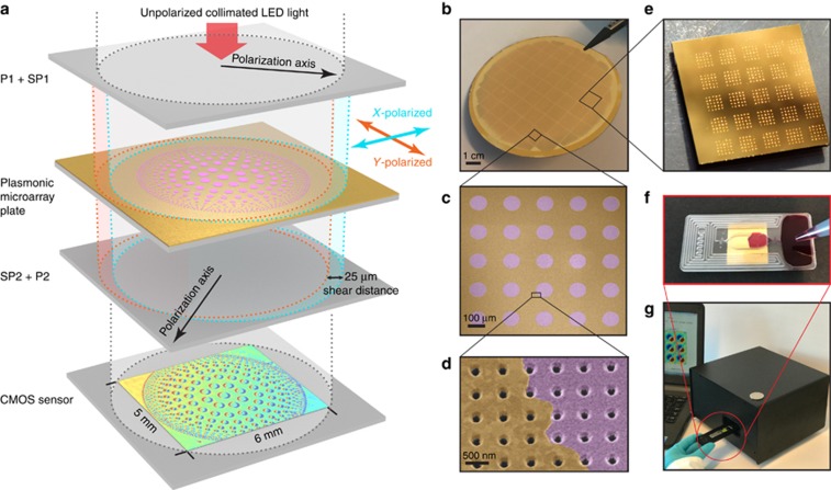
Figure 1.
Large FOV interferometric microarray imager (LIM) and experimental setup. (a) Collinear optical light-path configuration of the LIM setup. Collimated LED light beam is polarized (P1) and then sheared by a SP (SP1). This generates quasi-spatially overlapped and orthogonally polarized light beams that traverse the plasmonic microarray plate and are subsequently recombined using a second SP (SP2) and interfered by a second polarizer (P2). The interferogram is finally imaged by the CMOS sensor. The image shown on the schematic CMOS sensor is a real measured interferogram of a 10 nm-thin silica (SiO2) pattern on a plasmonic chip. (b) Photograph of a wafer comprising 1 cm × 1 cm plasmonic Au-NHA chips fabricated using high-throughput, wafer-scale nanofabrication tools. (c, d) Artificially colored scanning electron microscopy images of 10 nm thin silica microarrays on uniformly patterned plasmonic Au-NHAs. (e) Photograph of a plasmonic chip with 200 pl volume protein droplet microarrays formed using low-volume liquid dispensing tool. (f) Disposable capillarity-based microfluidic platform assembled on the plasmonic microarray plate. (g) Portable interferometric microarray imager operated through an interface running on an ordinary personal computer.

