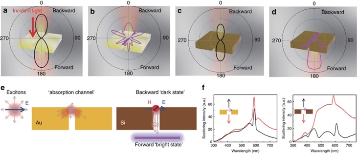
Figure 4.
Unidirectional ‘dark states’ in silicon NGs. (a) The schematic and calculated scattering pattern from a gold bi-pass NG with a thickness of 100 nm under the incident wavelength of λ=587 nm. (b) Schematic illustration and calculated scattering pattern of the Au NG-J-aggregate hybrid nanostructure. (c) Schematic illustration and calculated scattering pattern of a bi-pass Si NG under the incident wavelength of 587 nm. (d) Schematic illustration and calculated scattering pattern of the Si NG-J-aggregate hybrid nanostructure. (e) Schematic explains the ‘absorption channel’ in a gold-exciton hybrid system and the unidirectional ‘dark state’ in a silicon–exciton hybrid system. (f) Simulated backward and forward scattering from single-dipole emitter–NG hybrid systems.

