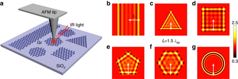
Figure 2.
Theoretical calculations of SP interference patterns in the two-dimensional graphene nanostructures. (a) Schematic showing the excitation and detection of the graphene SP waves using an AFM metalized tip. The graphene (Gr) nanostructures are fabricated on a SiO2 substrate. (b–f) Interference patterns of the graphene SP waves within the graphene nanostructures with two, three, four, five and six boundaries. The white double-headed arrows indicate the separation, L, between the centers and boundaries, which are fixed at 1.5λsp. (g) Interference pattern of the graphene SP waves in a circular nanostructure. The white double-headed arrow indicates the radius, which is set as 1.5λsp.

