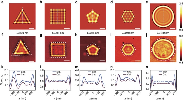
Figure 3.
Comparison of the experimental and theoretical results of the SP interference patterns in the two-dimensional graphene nanostructures. (a–e) Theoretical interference patterns of the graphene SP wave within the equilateral triangle, square, regular pentagon, regular hexagon and circular graphene nanostructures. SP wavelengths of 185 nm are used in the calculations, which correspond to an EF of 0.375 eV. (f–j) Corresponding experimental near-field amplitude images of the graphene nanostructures. The boundaries are indicated by the white dashed lines. (k–o) Extracted experimental (blue) and calculated (red) normalized amplitude profiles along the white dashed lines marked in a–e. The normalizations are performed by dividing the amplitudes of the nanostructures by that of the pristine SiO2 substrate. Scale bars=200 nm.

