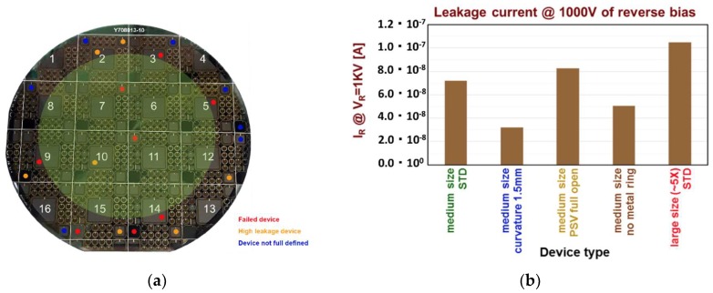
Figure 8.
(a) Image of a typical wafer with the indications of the failed and of the high-leakage devices. The majority of the failed devices are on the edge of the wafer where the majority of defects are present; (b) the leakage currents of the good devices do not show any dependence on the particular edge structure.

