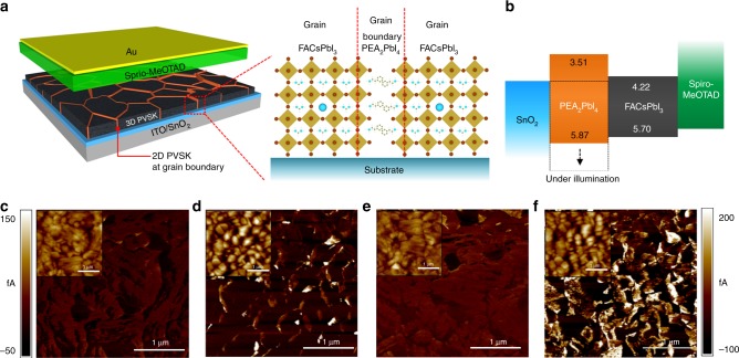
Fig. 4.
Band alignment and local conductivity with 2D perovskite. a Schematics of the device incorporating polycrystalline 3D perovskite film with 2D perovskite at grain boundaries and b band structure of each layer in device analyzed by ultraviolet photoelectron spectroscopy (UPS) and Tauc plots. Conductive atomic force microscopic (c-AFM) images of (c, e) bare FAPbI3 and (b, d) with 2D perovskite films on SnO2 coated ITO glass. The measurement was carried out with bias voltage of 100 mV under (c, d) room light or (d, f) low intensity light illumination provided by the AFM setup. Inset of each image shows corresponding topology of the films. Scale bar at left side is for (c) and (d) while at right side is for e and f

