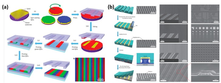
Figure 2.
(a) The processing steps of micro-contact printing. Functional materials on the modified surface could be adhered to the printing stamp, and then the functional materials are deposited on specific regions of surfaces. Functional material patterning formation. Reproduced from [44], with permission from Macmillan Publishers Ltd., 2011; (b) The processing steps of transfer printing. Left: Ink filling in the templates and transferring with a high-resolution. Right: Patterned functional micro-nano structure. Reproduced from [45], with permission from Macmillan Publishers Ltd., 2011.

