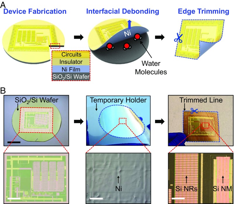
Fig. 1.
(A) Schematic illustrations of key steps for physically liberating a thin-film nanoelectronics from its fabrication SiO2/Si wafer in water. The Inset shows a cross-sectional illustration. (B) Optical images of the thin-film nanoelectronics on the SiO2/Si wafer (Left), and peeled with a thermally releasable tape (Middle), and then trimmed neatly (Right). (Scale bar: 2.5 cm.) The Bottom frame shows the corresponding microscope images. (Scale bars: 1 cm, 400 μm, and 300 μm, respectively.)

