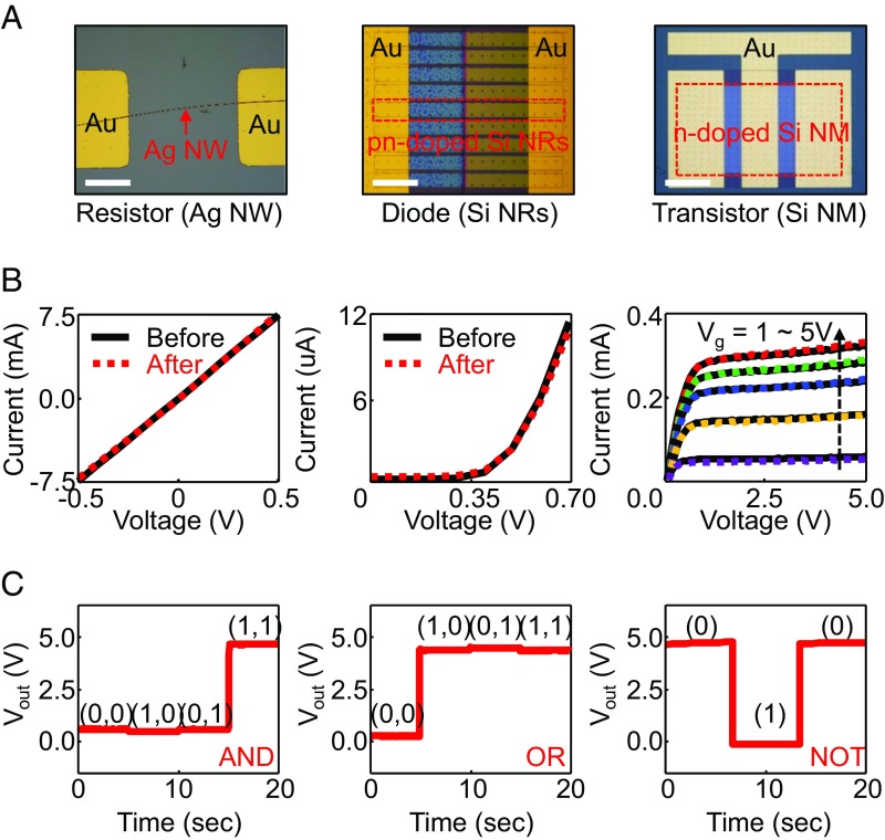
Fig. 3.
(A) Microscope images showing the transferred Ag NW-based resistor (Left), Si NRs-based p-i-n diode (Middle), and Si NM-based transistor (Right) on a piece of glass, each of which is transferred from its fabrication SiO2/Si wafer. (Scale bars: 40, 200, and 250 μm, respectively.) (B) Corresponding electrical characteristics to the each device before and after the transfer printing process. (C) Output voltage characteristics of AND (Left), OR (Middle), and NOT (Right) logic gates with Vin = 5 V.

