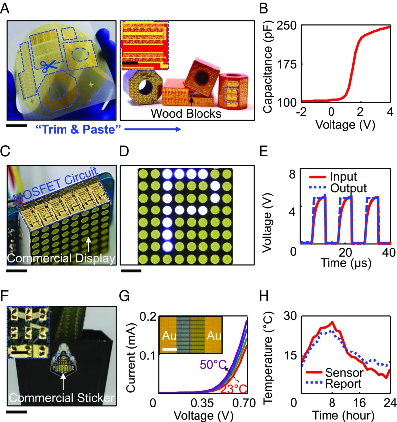
Fig. 4.
(A) Optical images of arrays of n-doped Si NM-based thin-film capacitors on a thermally releasable tape (Left) and after pasted on the surface of commercial wooden blocks with right fits (Right). (Scale bar: 2 cm.) The Inset shows a magnified view of the transferred devices. (B) Electrical characteristics of a representative capacitor in the arrays. (Scale bar: 2 mm.) (C) Optical image of arrays of n-doped Si NM-based MOSFETs pasted on the side wall of a commercial LED display. (Scale bar: 6 mm.) (D) Screen-captured image of the displayed letter “P.” (Scale bar: 4 mm.) (E) Measured clock signals switched by the transferred n-MOSFETs. (F) Optical image of arrays of pn-doped Si NRs-based temperature sensors pasted on the surface of a commercial flowerpot with a commercial sticker. (Scale bar: 2 cm.) The Inset shows a magnified view of the transferred sensor arrays. (Scale bar: 2 mm.) (G) Electrical characteristics of the Si NRs-based sensors with varied temperature ranging from 23 to 50 °C with a hot plate. The Inset shows an optical microscope image of the embedded Si NRs. (Scale bar: 150 μm.) (H) Measured environmental temperature obtained from the Si NRs-based sensor and a local weather report over a period of 24 h.

