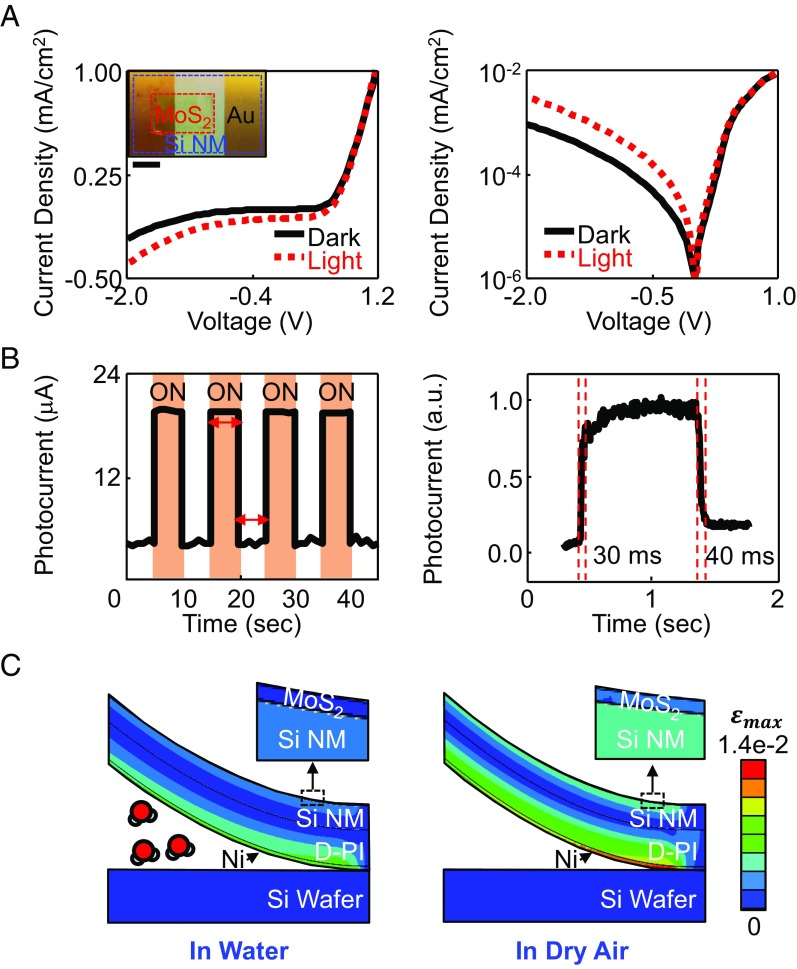
Fig. 5.
(A) Linear (Left) and logarithmic (Right) expression of current density–voltage (J–V) characteristics of a hybrid photodiode system that combines p-doped Si NM and n-doped MoS2 under dark and light conditions. The Inset shows a top view of the hybrid photodiode nanosystem. (Scale bar: 3 mm.) (B) Time-dependent on/off photoresponse in multiple (Left) and single (Right) light stimulation with external bias voltage of −2 V. (C) FEA results of maximum principle strain distributions in the thin films under mechanical peeling in water (Left) and dry air conditions (Right).

