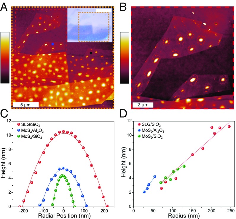
Fig. 1.
Interfacial blisters between 2D crystals and their supporting substrates. (A) Tapping-mode AFM reveals the complex distribution of HOPG-SiO2 blisters. (Inset) Bright-field optical micrograph where the orange dashed region corresponds with the large AFM image. (White scale bar: 10 μm.) The red, blue, and black dots indicate where Raman measurements were taken for SI Appendix, Fig. S2A. The color bar represents 0–17 nm. (B) A closer look at two monolayer regions from the red dashed region of Fig. 1A. Blisters close to the edges of the graphene are distorted from the typical circular shape. The color bar represents 0–13 nm. (C) By extracting the height profile of each blister, the height and radius is calculated by curve fitting a parabolic function. (D) Blisters for a specific interface show a consistent aspect ratio that is independent of volume.

