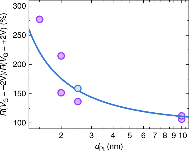
Fig. 3.

Thickness dependence of the Pt resistivity modulation. Dependence of the resistivity modulation factor k = R(VG = −2 V)/R(VG = +2 V) on the thickness of Pt layer dPt. Blue solid line shows theoretical calculation assuming the same number of carriers induced in all devices, as described in the main text; purple filled circles are experimental data, each circle corresponds to a separate sample. The blue filled circle is the averaged resistivity modulation k obtained for 2.5 nm sample from 15 gate voltage sweeps (see Supplementary Note 5 for details). In agreement with the theoretical calculation, devices showed increased resistivity modulation factor k with the decreased thickness. Note the logarithmic scale of x-axis
