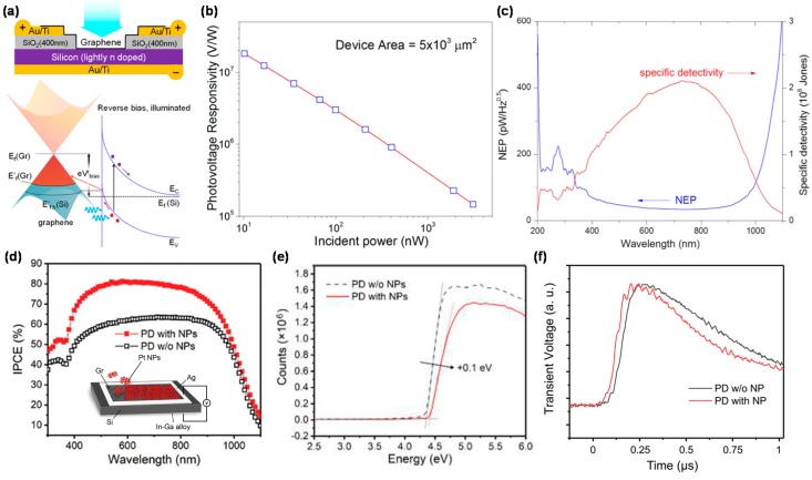
Figure 1.
(a) Schematic diagram and band structure of a typical monolayer graphene/Si heterojunction device. Application of a reverse bias raises Ef (graphene: Gr) and opens up a large number of accessible states that can be occupied by photoexcited holes injected from Si under illumination; (b) Variation of the voltage responsivity as a function of incident power, obtained under the open-circuit condition. At the lowest powers, the voltage responsivity exceeds 107 V/W; (c) Spectral dependence of the NEP and specific detectivity (D*) in the photocurrent mode. Reproduced with permission for Figure 1a–c from 2013 Nano Letter [24]; (d) Incident photon conversion efficiency (IPCE) spectra of graphene-Si PDs with and without fractal Pt NPs. The inset shows schematic diagram of a Si-graphene PD with fractal Pt NPs; (e) Ultraviolet photoelectron spectroscopy data of graphene-Si PDs with and without fractal Pt NPs, showing the effect of physical doping on the Fermi level; (f) Transient photovoltage characteristics of graphene-Si PDs with and without fractal Pt NPs under 532 nm pulse laser. Reproduced with permission for Figure 1d–f from 2017 Advanced Optical Materials [29].

