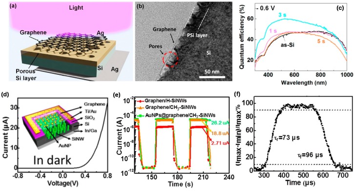
Figure 2.
(a) Schematic diagram of graphene/PSi/n-Si PD with silver top and bottom electrodes under light illumination; (b) Cross-sectional transmission electron microscopy (TEM) image of graphene/PSi junction; (c) Quantum efficiencies of as-Si, 1, 3, and 5 s PDs (Here, 1, 3, and 5 s mean the deposition time (td) of Ag nanoparticles. That is, the pore on the surface of the PSi increases as the time increases, Reproduced with permission for Figure 2a–c from 2014 ACS Applied Materials & Interfaces [35]; (d) Current-voltage curves of the Au NPs-graphene/SiNWs array PD. The inset shows the device structure; (e) Photoresponse of three representative devices under 850 nm light illumination at V = 0; (f) A single normalized cycle measured at 2200 Hz for estimating both rise time (tr) and fall time (tf). Reproduced with permission for Figure 2d–f from 2014 Scientific Reports [36].

