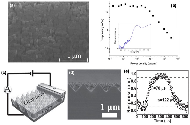
Figure 4.
(a) Scanning electron microscopy (SEM) image of a graphene film on GaN NWs; (b) Responsivity for various incident power densities. The inset shows the photocurrent spectrum of the PD. Reproduced with permission for Figure 4a,b from 2013 Applied Physics Letters [43]; (c) Schematic illustration of the graphene/GaAs nanocone array device; (d) A typical cross-sectional SEM image of the n-GaAs nanocones array after etching; (e) Single normalized cycle at 50 Hz to find both rise time (τr) and fall time (τf). Reproduced with permission for Figure 4c–e from 2014 Advanced Functional Materials [44].

