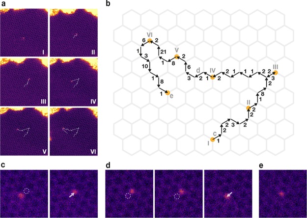
Figure 1.
Controlled electron-beam manipulation of a Si heteroatom in graphene (STEM images recorded with a MAADF detector). (a) Overviews where the segmented line indicates each of the 34 precisely directed lattice jumps and dots the locations of the Si atom in each previous panel (I–VI). (b) Schematic illustration of the path with orange circles indicating the position of the Si in each overview labeled with Roman numerals (I–VI) and with Arabic numerals indicating the number of 10 s spot irradiations required for each jump. (c) Closer views before and after the first jump. The location where the electron beam was parked is indicated by the dashed open circle. (d) Closer views of the two frames before and after the 20th jump. (e) Closer view near the end point of the sequence where a C atom has been knocked out, resulting in 4-fold-coordination of the Si.

