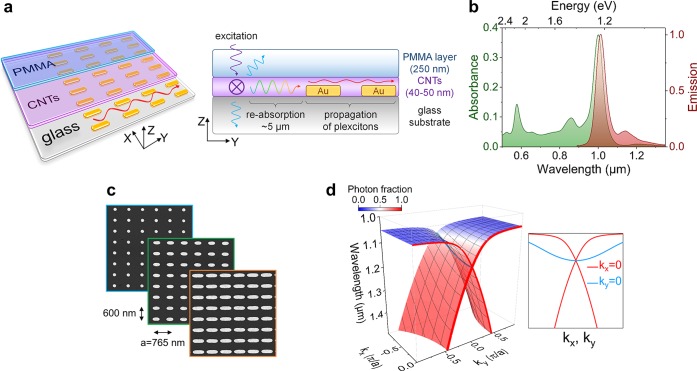
Figure 1.
(a) Schematic sample layout consisting of a glass substrate, plasmonic crystal, a layer of randomly in-plane oriented (6,5) CNTs and a PMMA film. The indirect excitation of plexcitons is performed via light emission from the carbon nanotubes pumped at a position 5 μm from the edge of the plasmonic crystal. (b) Absorption and photoluminescence spectra of a 40–50 nm thick film of (6,5) CNTs. (c) Scanning electron micrographs of gold nanodisks (diameter 165 nm) and two types of nanorods (380 × 180 nm and 620 × 200 nm). All plasmonic crystals have 765 nm pitch along the main propagation direction (Y-axis) and 600 nm in the orthogonal direction (X-axis). (d) 3D representation of the plexcitonic λ(kx, ky) dispersion. Color scale represents variation of photon and matter (excitonic + plasmonic) fractions. The inset compares the dispersion along X (ky = 0) and Y directions (kx = 0).

